Issue 025, January 25, 2022
Patrick K. Bowen, PhD, Director of R&D
Paliney 25 was introduced by Deringer-Ney in 2017. The new palladium-based alloy was a novel, high-performance material designed principally for the testing of integrated circuits (ICs). The performance of IC test alloys are essentially governed by: yield strength, both at room and elevated temperatures; bulk electrical conductivity; microhardness; and alloy nobility. A higher proportion of noble metal hinders the development of resistive surface films, thus decreasing the rate of contact resistance increase, and necessitating fewer cleanings in-service¹. The two-fold effect of increased alloy nobility is thus to (1) maintain a high yield (i.e. during wafer sort), and (2) extend touchdown lifetimes by minimizing abrasive cleaning. Increased popularity of elevated temperature chip testing also increases the probability of tarnish resulting from high temperature oxidation; a phenomenon also combatted through use of noble metals².
Susceptibility of the Paliney 25 alloy to tarnish by two common agents—oxygen and sulfur—was evaluated. Coupons were rolled to a thickness of 0.014 in (0.356 mm) and specimens were age hardened from both the cold worked (yielding “HTCW” temper) and annealed (“HTA”) conditions. A representative alloy microstructure is depicted in Figure 1. Samples were subjected to abrasion and final cleaning with isopropyl alcohol.
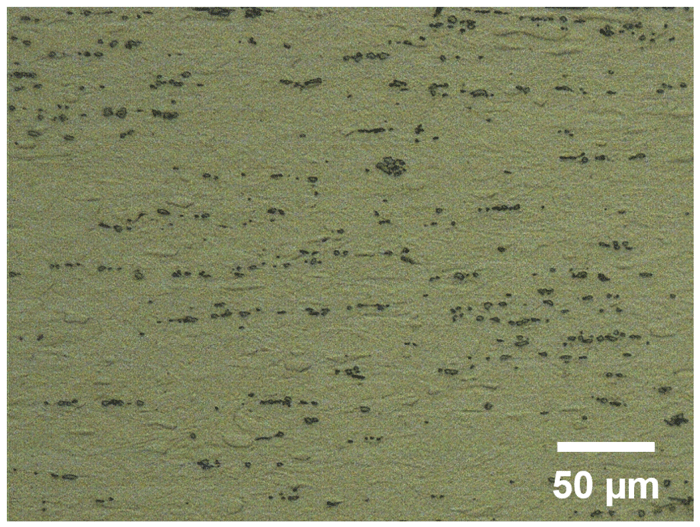
Figure 1: Representative microstructure of age hardened Paliney 25 coupons used for tarnish study.
Oxidation testing was performed in convection laboratory ovens maintained at 50, 125, and 150°C. Sulfidation testing was performed in a glass vessel kept at 79% relative humidity and 50°C, with coupons suspended above crystalline sulfur. Sulfurous atmospheres are known to stimulate the formation of both copper and silver sulfides³. Contact resistance was measured under a 31 gf load applied over a 0.100 in (2.54 mm) radius Neyoro™ G probe. Measurement utilized a precision, 4-wire multi-meter operated in dry circuit test mode.
Measurements, less the 125°C condition for brevity, are shown in Figure 2. From Figure 2(A) it is observed that exposure to the humid, sulfur-containing environment instigated a rapid rise in Paliney 25 contact resistance, which then stabilized after the first ~100 hours. Results of the 50°C and 150°C oxidation tests, in Figure 2(B) and (C), respectively, demonstrate the expected temperature dependence of contact resistance rise. Exposure to 50°C temperatures produced no change in contact resistance, with measured contact resistances below about 10 mΩ for the duration of the test. In marked contrast, exposure to 150°C caused a monotonic increase to an observed maximum of 113 ± 51 mΩ at 2,000 h. At longer times, a decrease was observed. This is generally attributed to loss of coherency of the oxide film, which allows the indenter to move aside the resistive tarnish products under applied load.

Figure 2: Paliney 25 contact resistance in sulfurous (A); 50°C oxidizing (B); and 150°C oxidizing (C) environments. Shaded areas represent the sample standard deviation. Note differences in X- and Y-axes between plots.
A contact resistance “map” was compiled using the test data, shown in Figure 3. The figure shows approximately the extremes of contact resistance that can be expected for Paliney 25 over the time and temperature range examined in this work.
Two tarnish-related performance attributes of Paliney 25 for IC test probes can be extracted from this work. First, the alloy is shelf stable, maintaining near-virgin contact resistances even after extended exposure to 50°C temperatures. Second, the slow, steady increase of contact resistance at temperatures up to 150°C suggests that the material is well suited to hot-chuck testing applications. While non-noble metals may require frequent abrasion to remove oxides, Paliney 25 would require only infrequent service. (Contact resistance of non-noble metals are discussed in Pitney⁴.) This critical capability makes Paliney 25 appealing for cutting-edge IC testing in applications like on-board charging, motor control, high power DC/DC conversion, and other high temperature devices.

Figure 3: Schematic contact resistance map for Paliney 25.
Note: Paliney® is a registered trademark of Deringer-Ney Inc. Paliney 25 is protected by US patent 11,041,228 and family.
References:
[1] J. Broz, G. Humphrey, and W. Fitzgerald, “Probe Card Cleaning ‘A Short Tutorial,’” San Diego, CA, USA, Jun. 2007. [Online]. Available: https://www.swtest.org/swtw_library/2007proc/PDF/T00_01_Broz_SWTW2007.pdf
[2] M. Takahashi and G. Franz, “High Temperature Wafer Probing of Power Devices,” presented at the IEEE Semiconductor Wafer Test Workshop 2019, Jun. 2019. [Online]. Available: https://www.swtest.org/swtw_library/2019proc/PDF/S05_03_Takahashi+Franz_SWTest_2019.pdf
[3] T. E. Graedel, J. P. Franey, G. J. Gualtieri, G. W. Kammlott, and D. L. Malm, “On the mechanism of silver and copper sulfidation by atmospheric H2S and OCS,” Corrosion Science, vol. 25, no. 12, pp. 1163–1180, 1985
[4] K. E. Pitney, Ney Contact Manual: Electrical Contacts for Low Energy Uses. Bloomfield, Connecticut: The J. M. Ney Company, 1973. [Online]. Available: https://www.deringerney.com/publications/ney_electrical_contact_manual/