Issue 050, Sept 4, 2023
Wade A. Jensen, Ph.D., Sr. Research Metallurgist
Metals are commonly used in electrical systems due to their high electrical conductivity, with the most conductive being Cu, Ag, and Au. Electrical conductivity can be explained simply by the free electron model. This states that metals consist of periodic array of atoms, each with valence electrons that can dissociate and move freely in the lattice. This creates a “sea of electrons” that, when a voltage (electrical potential difference) is applied, results in electron migration towards the positive terminal. Defects in periodicity scatter electrons from their path; this process is random but gives rise to the macroscopic property of electrical resistance (the mathematical inverse of electrical conductivity). Engineering for low-resistance/high-strength materials is nontrivial as strengthening mechanisms¹ inherently increase electron scattering.
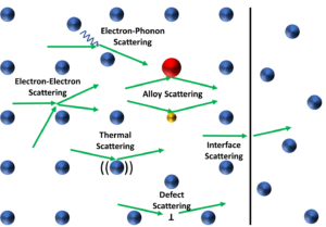
Figure 1: Diagram depicting an atomic lattice with examples of electron scattering
events. Electrons and their pathways are green.
Electrical resistance of a system can be understood through Matthiessen’s rule. This rule posits that every metal has an ideal, characteristic resistivity and partial resistivities that arise from categories of scattering events². The sum of these individual resistivity contributions gives the total resistivity for the system. Matthiessen’s rule can be expressed mathematically as:
![]()
Equation 1
Where ρ0 is the resistance of an ideal single crystal at 0°C, ρ(T)Thermal is the sum of scattering caused by thermal vibrations, ρAlloy is the scattering caused by substitutional or interstitial atoms, and ρInterface is the resistivity of all interfaces such as grain boundaries or interphase interfaces. Other contributions can be considered, such as: electron-electron scattering, electron-phonon scattering, defect scattering, etc. These will not be discussed here.
Thermal Scattering – As electrons travel through the lattice, collisions naturally occur between electrons and atoms. Temperature controls the degree of atomic vibrations around their lattice sites; materials at high temperatures have greater atomic vibrations and are more effective at scattering electrons, while low temperatures reduce vibrations and improve electron flow. As can be seen in Figure 2, electrical conductivity varies slightly over everyday temperatures, but the effects are significant at temperature extremes³.
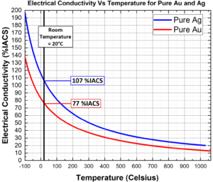
Figure 2: Plot showing the effects of temperature on the electrical conductivities of Ag (blue)
and Au (red). Parameters and equations were taken from³.
Alloy Scattering – Also known as impurity scattering, this resistance is based on scattering caused by substitutional or interstitial alloying. As can be seen in Figure 3, Ag is an exceptional electrical conductor, however its softness excludes it from many applications. Ag can be alloyed with Au to produce a harder alloy. Even though Au is also an excellent conductor, the combination significantly reduces conductivity. 10% Au is sufficient to reduce Ag conductivity from ~107 to ~34 %IACS. For some solute saturated systems, precipitation of a secondary phase would reduce impurity concentrations in the metal matrix and improve electrical conductivity.
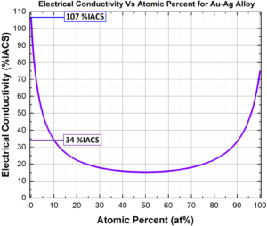
Figure 3: Plot showing the effects of alloying on the electrical conductivities of
Ag-Au alloy (purple). Parameters and equations were taken from³.
Interface Scattering – Two common types of interfaces found in metals are grain boundaries and interphase interfaces (boundary between two phases). Both interfaces are discontinuities in the periodic lattice and similarly scatter electrons, but only grain boundaries will be discussed here. Figure 4.a) shows the effects of interface collective density on Cu conductivity⁴; once the spacing between grain boundaries is smaller than 1 μm, the grain boundaries become a significant scattering contributor. This can be seen visually in 4.b), which depicts a Cu lamellar grain structure with yellow grain boundaries. The width of the interface is the same for all images, but with decreasing Cu width the interfaces begin to dominant and the diagram appears more yellow. The individual contribution of a single interface is insignificant, but copious interfaces can contribute to significant scattering.
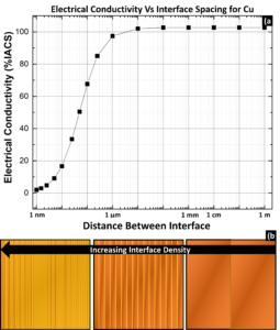
Figure 4: a) Plot showing the effects of interface spacing (and therefore interface density) on electrical conductivity for Cu. Parameters and equations were taken from⁴. b) diagram depicting grain boundaries (yellow) and the effects of decreased spacing.
Deringer-Ney is experience at making noble alloys with a range of hardness and conductivity, so that our customers can select high quality products that fit their application’s need.
Paliney® and Neyoro™ are registered trademarks of Deringer-Ney Inc.
References:
- W. Jensen, Tech Brief 028 – How to Interpret Binary Alloy Phase Diagrams, in: Deringer-Ney Tech
Brief, 2022. https://deringerney.com/how-to-interpret-binary-alloy-phase-diagrams/. - F.C. Schwerer, J.W. Conroy, S. Arajs, Matthiessen’s rule and the electrical resistivity of iron-silicon
solid solutions, Journal of Physics and Chemistry of Solids. 30 (1969) 1513–1525. https://doi.org/10.1016/0022-3697(69)90213-3. - V.K. Iyer, R.M. Asimow, The electrical resistivity of gold-silver alloys, Journal of the Less Common
Metals. 13 (1967) 18–23. https://doi.org/10.1016/0022-5088(67)90043-4. - I. Bakonyi, Accounting for the resistivity contribution of grain boundaries in metals: critical analysis of reported experimental and theoretical data for Ni and Cu, Eur. Phys. J. Plus. 136 (2021) 410.
https://doi.org/10.1140/epjp/s13360-021-01303-4.