Did you know that semiconductor testing represents approximately 20-25% of chip manufacturing cost? To help remedy this, manufacturers are constantly looking for ways to improve efficiency to reduce testing costs while simultaneously meeting the demands of new chip designs. This is where the foil probe comes in. These precision-engineered devices help deliver much needed flexibility and improved accuracy for semiconductor quality assurance. Today, we will discuss the evolution of testing probes and the benefits of palladium alloy foil probes.
Historical Evolution and Material Innovation
Buckling beam probes have been the standard since the 1970’s. They rely on a beam-like structure containing many thin wires that bends under pressure. The wires are typically made from Pd-Ag-Cu-based alloys but have their limitations due to their rigidity and other factors.
Times have changed, and so has probe technology. In a departure from traditional methods involving wire, pins or electrodeposited MEMS, laser-cut foil probes can be made directly from thin metal sheets. This innovation has expanded material choices and design possibilities, though it also raised questions about material property performance across different orientations.
Foil Probes and Their Applications
Foil probes are ultra-thin metal sheets that function as both electrical conductors and precision contact elements in semiconductor testing applications. These components are integral parts of probers—testing tools that verify the functionality of semiconductor devices while still on the wafer, before being cut into individual chips. Operating at microscopic scales, these probes must maintain precise positioning at pitches as small as 100-150 micrometers while functioning as self-contained electrical conductors and spring members.
Technical Advantages and Material Properties
The move to foil-based designs brings multiple advantages over traditional wire probes and electroformed MEMS alternatives. MEMS manufacturing usually restricts materials to pure metals via electroplating, while foil probes can employ precious metal alloys that combine many beneficial properties. Of particular importance is the use of noble metals such as palladium, which provides the required spring characteristics and sustained conductivity without oxidation issues.
Anisotropy in Foil Applications
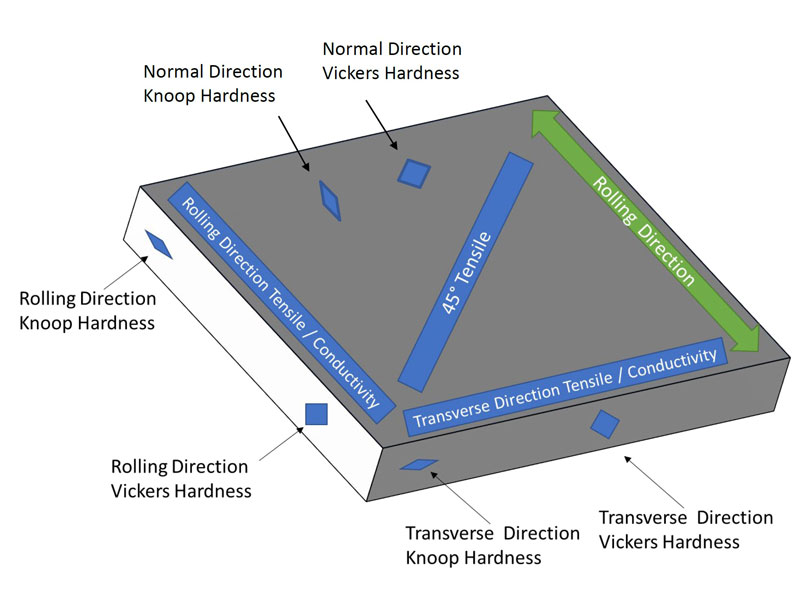
Recent material research for probes by Deringer Ney has centered on learning about the anisotropy—directional dependence—of material properties of palladium alloy foils. Extensive testing of 50μm thick foils was performed using two Pd-Cu-Ag-based compositions, evaluating properties in several orientations relative to the rolling direction. The study included tensile strength and yield behavior, microhardness measurements, and electrical conductivity testing.
The results were both surprising and promising: the Pd alloy foils presented high strength and virtually no anisotropy in all the tested orientations. Tensile properties and hardness were independent of direction, with stress-strain behaviors appearing very consistent. This is good news. Isotropy, or direction independence, is a great benefit for probe designing and manufacturing. It removes the limits of traditional methods, while bringing significantly increased flexibility and efficiency.
Why This Matters: Impact on Semiconductor Testing
These findings have implications that go beyond material science. In testing semiconductors, a probe card must interface with either metal pads or solder bumps on the surface of a wafer, which puts a premium on precise positioning and reliable electrical contact. The proven isotropy of palladium alloy foils allows for more complex probe designs, such as crisscrossing features and structures running at a variety of angles-a critical time-saving advantage to help meet today’s testing requirements.
The combination of higher hardness and excellent electrical conductivity in alloys like Paliney 23 (sometimes abbreviated P23 in semiconductor test) and Paliney 25 (P25) allows for reduced cross-sections while maintaining performance. This enables testing at tighter pitches, critical for the industry’s push toward increasingly miniaturized semiconductor devices.
What’s Next?
The semiconductor industry will certainly continue its relentless drive toward miniaturization, with testing technology working to keep pace. While wire probe technology has evolved significantly over five decades, foil probe innovation represents the next phase in testing capability. The development and refinement of specialized alloys remain key to advancing this technology.
Materials innovation becomes ever more critical as semiconductor manufacturers push towards smaller test pitches with ever-more-demanding test requirements. Success in palladium alloy foil probes shows that material science can help solve complex challenges, while pushing design and innovation forward.
Conclusion
The emergence of palladium alloy foil probes represents a significant advancement in semiconductor testing technology. Their unique combination of mechanical properties, reliability, and design flexibility—particularly their unexpected isotropy—provides semiconductor manufacturers with new tools to address the challenges of modern chip testing. As the industry continues to evolve, innovations in materials and probe design will continue to play an increasingly enabling role in the next generation of semiconductor devices.